PCB Quality Inspection
PCB Quality Inspection
Become a customer to access all support documents.
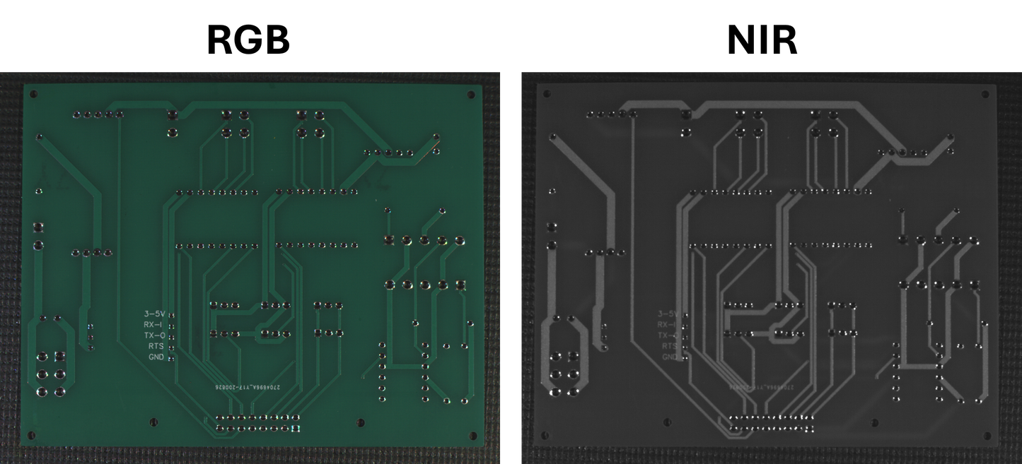
Printed circuit board (PCBs) quality can be inspected using multispectral imaging. PCBs consist of copper wires (traces) laminated into a substrate, such as fiberglass, and sandwiched between a solder mask. Inspection of the traces allows for identification of copper under or over etching, which can cause malfunction of the PCB by introducing shorts or incomplete traces.
An image of a PCB was taken using a MSLED-RGBN-2-4 illuminator with four spectral channels (red (620 nm), green (520 nm), blue (470 nm), near-infrared (850 nm)) and a monochrome 4.2 MP camera, MSC2-M42-1-A. The images obtained using red, green and blue light were merged to form a typical color (RGB) image.
The copper traces can be seen in the RGB image, however, due to higher penetration of longer wavelengths and higher copper reflectance in near-infrared (NIR) range the traces underneath the solder mask are more clearly visible in the NIR image.


